Photolithography: The Art of Writing with Light
Giroscience Scientific Review Team
12/21/20251 min read

What if we could etch features smaller than a virus onto silicon, pushing computing power to unimaginable new limits?
That's the ongoing revolution of photolithography.
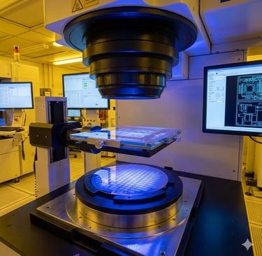
Photolithography is the core technology enabling modern electronics, essentially "printing" microscopic circuit patterns onto silicon wafers using light.
A wafer is coated with photoresist, a light-sensitive material. A patterned mask acts as a stencil, and intense light (typically UV or Extreme Ultraviolet - EUV) shines through, selectively changing the photoresist.
The exposed areas are then developed, creating a protective pattern. This pattern guides subsequent etching or material deposition steps, building up complex 3D circuits layer by layer.
Recent breakthroughs, particularly in EUV lithography led by companies like ASML, use incredibly short wavelengths (13.5 nm) to print features as small as 2 nm, allowing billions of transistors on a single chip.
This relentless miniaturization drives everything from AI to advanced sensors, promising a future where computing power is vastly more integrated and transformative in our daily lives.
Learn more: https://www.asml.com/en/technology/lithography-principles
👉 Follow @giroscience for more science and knowledge!
🌌🧠 All rights and credits reserved to the respective owner.
Image: Ai Generated.
Get Your Printed Art
Enhance the ambiance of your home or office with the timeless charm of a beautifully framed print
Buy a framed Art Print of my illustration on my Redbubble Shop
© 2025. All rights reserved.
Disclaimer: While browsing our website, you may encounter affiliate links, as well as direct links to our own platforms where you can purchase our digital illustrations, products featuring our designs, or other science-related products.If you click on an affiliate link and make a purchase, we may earn a small commission at no additional cost to you. We only recommend products and services that we genuinely believe in and that align with our brand and values. Thank you for your support—it helps us continue creating content!